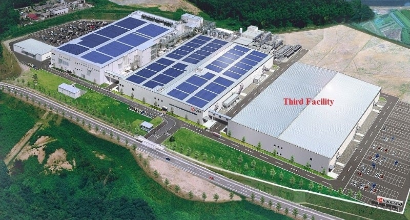
Japanese multinational electronics and ceramics manufacturer Kyocera Corporation began construction of a new manufacturing facility at its existing Kyoto Ayabe complex in Ayabe City, Kyoto, in April 2016.
Kyocera’s third facility at the complex will strategically expand the company’s production capabilities of organic packages for microelectronic devices.
The new plant will commence operations in April 2017.
Project background
Kyocera is investing in the new facility to meet the expected growth for its packaging products due to the increasing demand for consumer devices that incorporate multiple internal modules for camera, wireless, power amplifier and control functions.
The company also sees an opportunity from the expanding internet of things (IoT), which is expected to provide new applications for its products. Microelectronic devices such as wireless and sensor chips are increasingly being used in packaging solutions based on organic material technology.
Details of Kyocera’s new manufacturing facility
The new production facility will have a built area of 13,143m² and 25,420m² of floor space. It will be a two-storey building embedded in steel frames.
The building is designed with environment-friendly features such as wastewater recycling systems for reusing water emissions.
Production at Kyocera’s new facility
The new plant will manufacture miniaturised, low-profile organic packages used for packing microelectronic devices used inside smartphones, tablet PCs and other telecommunications devices.
The microelectronic packaging products provide higher functionality, greater integration and slimmer designs in mobile communications equipment.
Kyoto Ayabe Complex details
The Kyoto Ayabe complex was constructed in 2005 and manufactures a wide variety of organic packaging products such as flip-chip ball grid array (FC-BGA) substrates for high-end application-specific integrated circuits (ASICs).
Over the course of time, the latest, high-end technologies have been added to the complex, including high-density wiring and automated production processes, to create smaller and lower-profile products.
Until March 2016, the complex was operated by the former Kyocera Circuit Solutions (KCS), a wholly owned subsidiary of Kyocera, specialising in high-density organic wiring boards, packages and large-scale printed motherboards for semiconductor devices.
KCS was merged into Kyocera Corporation on 1 April 2016, resulting in the transfer of the complex’s operating rights to the parent company. The merger was a part of business integration strategy to support the development of new products and markets, while further expanding business synergies.
The second facility at the Kyoto Ayabe complex was constructed in mid-2014. It involves manufacturing smaller, lower profile, flip-chip chip scale packaging (FC-CSP) for use in smartphones and tablet PCs. The plant is targeted to eventually reach an annual production of JPY20bn ($282m).
Marketing commentary on Kyocera
Situated in Kyoto, Kyocera Corporation was established in 1959. The company produces fine ceramics, combines them with metals, and integrates them with other technologies. It also manufactures solar power generating systems, telecommunication equipment, office document imaging equipment, electronic components, semi-conductor packages, cutting tools and components for medical and dental implant systems.


