
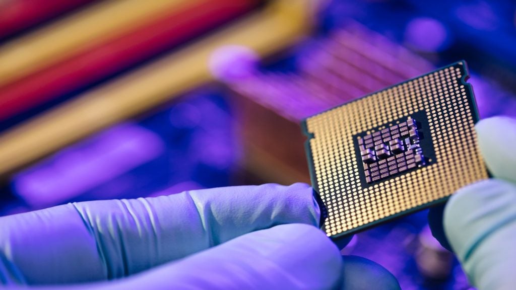
Japanese semiconductor materials manufacturer Resonac has confirmed its plans to set up a new Packaging Solution Center (PSC) for semiconductors in Silicon Valley, California, US.
This PSC will serve as a research and development (R&D) hub for semiconductor packaging technologies and materials.
Resonac said it has already commenced the preparation, investigation, and selection processes related to different facilities that will be equipped in the R&D centre.
Operations at the new centre are expected to start in 2025, after the company completes the installation of a clean room and required equipment.
The latest move builds on Resonac’s strategy to expedite the development of various technologies outside its home country.
Resonac said it intends to expand its presence specifically in a region where business bases of major semiconductor manufacturers and technology companies such as Google, Apple, Facebook, and Amazon, are located.
The company also has a PSC in Shin-Kawasaki, Japan, which is the first PSC established by Resonac.
This semiconductor packaging centre is equipped with various facilities, including laser dicing, fine wiring formation, and handling processes, as well as materials for 2.xD and 3D semiconductor packaging technologies.
All these facilities help in processing large-sized materials, including 300mm wafers and 500mm square panels.
According to Resonanc, its first PSC in Shin-Kawasaki has been serving as a 'one-stop hub' for all its trial implementation and evaluations related to production technologies and materials.
To further expand its offerings and technologies, the company said it is now planning to leverage its new PSC in the US to capture the real-time trends and concepts in packaging technology for semiconductors such as AI semiconductors.
The company will then utilise these latest packaging concepts to support the development of new materials.
In May 2022, Japanese company MITSUI MINING & SMELTING announced the opening of a new facility to manufacture its speciality carrier for semiconductor packaging.